Eched Wafer (CW) process
STC slices cylinder shape ingot to wafer shape, then treat outer shape by beveling process.After that rough polishing on wafer surface by lapping process. To reduce distortion by using ething process. To remove oxygen (Donar killer)from wafer by annealing process.
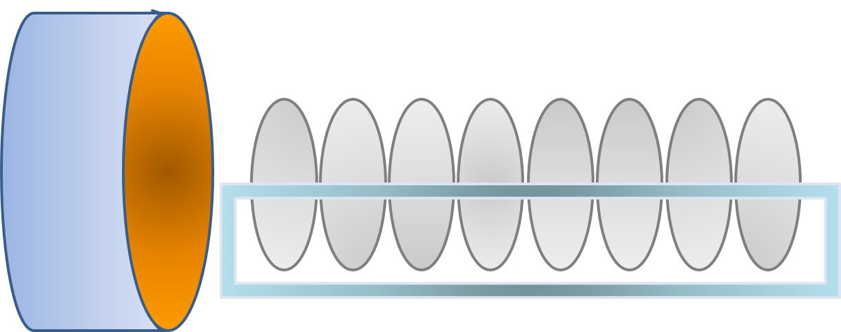
Slicing
Cylinder shaped ingot will be cut into wafer shape by inner blade cutter or wire saw cutter.
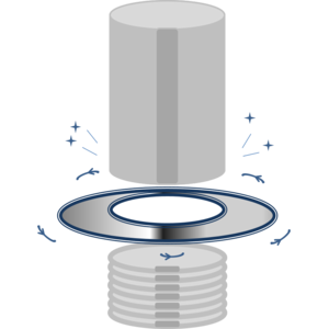
Beveling
Outer edge of sliced wafer is sharp. So, in order to preventing chipping at post processes, or generating particles after polishing process, beveling process will be needed and make it proper diameter at same timing.
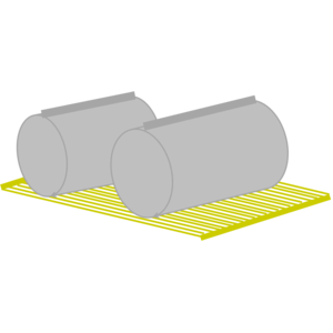
Lapping
Since there are micro convex/concave parts on wafer surface, the wafers are pinched by upper and lower high flatness disc then polish with pressure for making the wafer proper thickness.

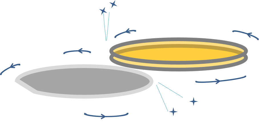
Etching
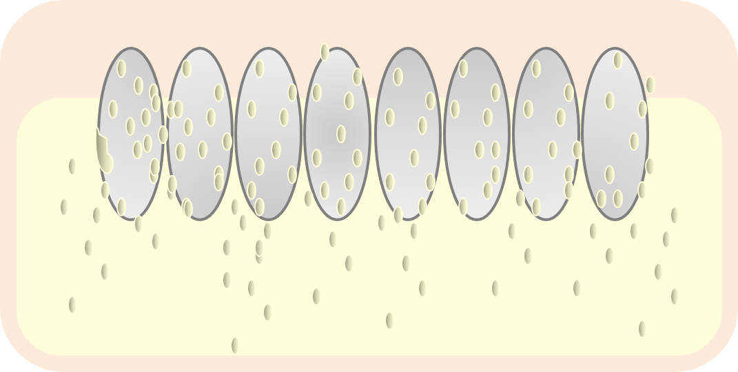
Since slicing, beveling, and lapping processes are mechanically processed, many deformations will be existed on silicon surface. In order to remove these deformations, STC uses chemical etching process.
Annealing
During the process of single crystallization by CZ method, few oxygen will be generated from quartz pod and mixed together to the crystal. In order to get stable resistivity value, STC puts the wafers into high temperature furnace and rapidly cooling which process we call donar killer.