Ultra High Flatness Wafer
Product Information
STC has succeeded in manufacturing single crystal silicon substrate, which has a high flat value even in small diameter. Usually, the limit of TTV is around 3um in small diameter, but STC has exceeded its limit and accomplished better than 1um. STC will also apply better flatness quality as per the customer’s requirements.
Ultra-High Flatness Wafer can be used for the base substrate, which is applicable for bonding or photolithography processes, and will fit for good uniformity based on several deposition processes, which means proper substrate for accuracy demanded several devices.
Also, a substrate manufacturer, STC, can make them in requested substrate thickness, an asymmetrical edge from ingot basis.We can support reducing customer’s power of process management, time, cost, and improving yield rate.
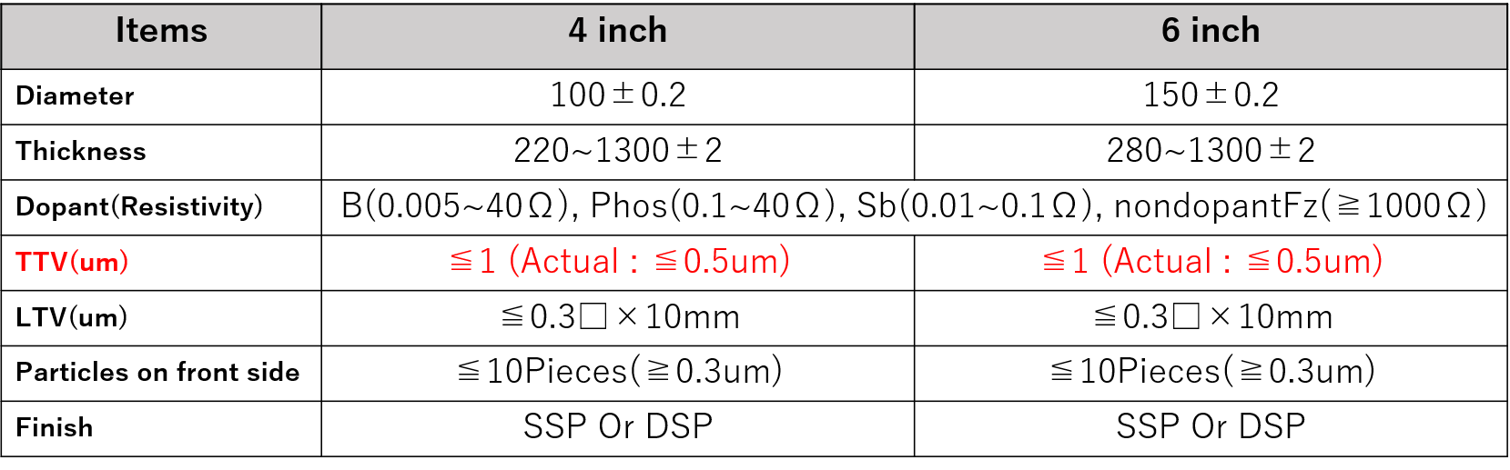
◎Standard Products Spec
- Dia:4, 6 inch
- TTV:≤1um(Actual:≤0.5um)
- Type:P(B),N(Phos,Sb),FZ
- Orientation:<100>,<110>,<111>
- Resistivity: ≤0.005 ~ 40 Ωcm
- Finish:SSP,DSP
◎Main Application
- Substrate for bonding
(SOI・LT・TC-SAW etc) - Substrate for Photo-Lithography
- Process which needs good TTV as important parameter.
◎Effective Case
- To reduce time and cost for thinning, also to be good flatness to substrates for bonding
- To improve the yield rate of wafer outer area to the edge
<Process Specification>
※Other options. Please ASK.
- Enlarge diameter (101,151mm) for SOI terrace free.
- Additional oxide layer process for BOX layer
- Notch type instead of flat shape
- Non Dope≥1000Ω(FZ)
Furthermore, STC can apply on the sample customized substrate for customer's R&D phase.